![<?echo $_SERVER['SERVER_NAME'];?>](/template/twentyseventeen/skin/images/header.jpg)
Abstract: An energy-saving video surveillance terminal is designed. The terminal is based on the TMS320DM642 chip. With the help of peripheral chips such as camera, image decoding chip TVP5150 and infrared sensor, the terminal can effectively monitor the access of regional personnel, and only start video image acquisition and processing when someone enters the monitoring area. , transmission, etc., not only achieve the purpose of monitoring, but also save some of the power.
Video surveillance systems are increasingly entering people's lives. System energy conservation is also an important parameter that electronic systems must consider. For an occasion where there are few people coming in and out, the use of uninterrupted real-time monitoring is not only unnecessary, but also wastes a lot of power. In response to this situation, this paper designed an unattended intelligent monitoring terminal. When no one enters the monitoring area, the monitoring terminal is in a low-energy sleep state; when the infrared sensor detects that someone enters the monitoring area, the terminal is woken up and starts to shoot, and the processed video signal is transmitted to the monitoring center through the network, The central duty officer provides the basis for judgment. For occasions with fewer people entering and leaving, the monitoring terminal can effectively reduce system energy consumption, reduce the amount of data transmitted and saved, and not miss the monitoring object.
1 Terminal working principle and overall block diagram
The overall block diagram of the terminal is shown in Figure 1. When no personnel enters the monitoring area, the system is in a dormant, energy-saving state. When the infrared sensor detects that a person enters the monitoring area, an external interrupt is generated, and the central processor TMS320DM642 receives an external interrupt. Immediately start each module to collect, process, and transfer images.
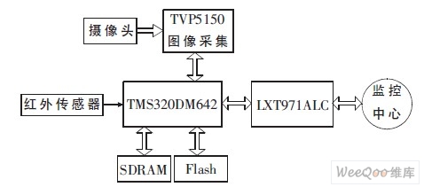
Figure 1 terminal block diagram
2 terminal system design
2.1 Central processor selection
Because the amount of data to be processed by the terminal is large and the real-time performance is strong, the multimedia processing chip TMS320DM642 (hereinafter referred to as DM642) is used. The chip is a newer 32-bit fixed-point DSP from TI's C6000 series of DSPs. The operating frequency is set by the internal multiplier, which can reach 500 MHz, 600 MHz or 720 MHz. The number of executable instructions per second is 4 000 , 4 800 , 5 . 760 MIPS. The DM642 uses TI's 2nd generation enhanced ultra-long instruction set. Its EMIFA interface has a data bus width of 64 bits and a maximum access frequency of 133 MHz. It can be directly connected to high-capacity, low-cost SDRAM chips. The DM642 features three dual-channel (A, B two-channel) digital video ports that can handle multiple digital video streams simultaneously. The DM642 has an I 2 C interface that can communicate with external I 2 C devices to configure external I 2 C device registers, the DM642's network port (EMAC interface), PCI port, and HPI port shared pins. Because of its strong processing performance, the peripheral interface is flexible and flexible, and has been widely used in machine vision, medical imaging, network video surveillance, digital broadcasting and other fields.
2.2 Design of infrared sensor signal processing module
In order to save power, the terminal uses an infrared sensor to detect whether there is a person entering the monitoring area. Only when a person enters the monitoring area, the terminal enters the image acquisition, processing, and transmission state. This design uses BISS0001 chip as the core component of pyroelectric infrared sensing signal processing. Its application circuit is shown in Figure 2.
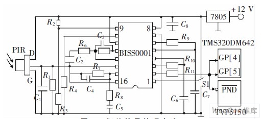
Figure 2 infrared signal processing circuit
In Figure 2, the 7805 is a three-terminal regulator IC that supplies power to the signal processing circuitry. The 9th pin of the BISS0001 chip is the input pin of the trigger control signal Vc. The input voltage Vc>VR should be guaranteed during operation (usually:
VR = 0.2VCC), can be achieved by adjusting the resistor R3. When a pedestrian enters the monitoring area, the pyroelectric infrared sensor PIR converts the detected infrared light emitted by the human body into an electrical signal, and sends it to the BISS0001. The signal is processed by the BISS0001 and output by the 2 pin. The output Vo is low. A flat to high transition. If BISS0001 works in the case where the active state cannot be repeatedly triggered (ie, S1 is connected to low level in Figure 2), the duration of the high level is Ts (Ts=49 152 R1C1). At the end of the Ts period, the output Vo is immediately When the high level enters the low level and is blocked by Ti (Ti = 24R2C2); for the case where the active state can be repeatedly triggered (ie, S1 is connected to the high level in Figure 2), if it is within the previous Ts period, The change in the input causes the output active state to trigger again, and the Vo high level signal will continue for a Tx period from the moment and then transition to a low level and enter the blocking time Ti. During the lockout time, even the interference introduced due to the switching of the load does not change the state of the output Vo. In this design, S1 is connected to a high level, and the output signal Vo of the infrared sensing signal processing circuit is used as an external interrupt signal of the DM642, and the GP of the Vo and DM642 [5:4]
Connected, and also used as the power-saving mode input control signal of the TVP5150 chip, as shown in Figure 2.
2.3 Image acquisition module design
For the image acquisition module, this design uses TI's TVP5150 as the decoding chip. The TVP5150 is an ultra-low power decoding chip that consumes only 113 mW during normal operation and 1 mW in power-saving mode. It supports PAL/NTSC/SECAM formats and can capture the camera. The analog image signal is converted into an ITU-R BT.656 digital signal in the YUV4:2:2 format, which can receive 2 composite video signals (CVBS) or 1 S-Video signal, and set internal registers through the I 2 C bus. Select to output 8-bit 4:2:2 ITU-R BT.656 digital signal (synchronous signal embedded), and 8-bit 4:2:2 ITU-R BT.601 signal (synchronous signal separation, separate pin output ). The hardware connection between TVP5150 and DM642 is shown in Figure 3.
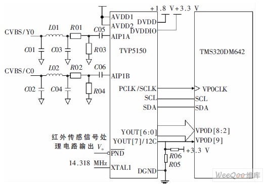
Figure 3 TVP5150 and DM642 hardware connection diagram
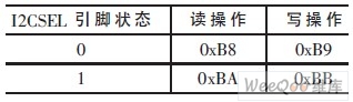
The AIP1A and AIP1B of the TVP5150 chip are the input terminals of the analog signal. This pin needs to be connected with a 0.1~1 μF filter capacitor. HSYNC is the output pin of the line sync signal. Since this design uses the ITU-R BT.656 format embedded in the sync signal, this pin is not connected to the DM642 related pin. The PND pin is the control signal input terminal of the power saving mode, and is active low. It is connected with the output signal Vo of the infrared sensing signal processing circuit. When there is no pedestrian walking in the monitoring area, Vo is low, which will make the TVP5150 chip. Enter the power saving mode. YOUT[6:0] is the BT.656/YUV data output pin, YOUT [7]/I 2 CSEL is the 7th bit of BT.656/YUV data, also the I 2 C interface device address setting bit, TVP5150 device address pull-up resistor or a pull-down resistor connected to the pin I 2 CSEL determination, the state of the I 2 CSEL pin device, address mapping is shown in table 1, the address from the sheet TVP5150 TVP5150 DM642 and response procedure requires. SCL and SDA are the serial clock and data pins of the I 2 C interface, respectively. The access of the DM642 to the TVP5150 internal registers is realized by the I 2 C bus.
VP0D [19:0] of DM642 chip is the data bus pin of video port VP0, where VP0D [8:2] is multiplexed with multi-channel serial port McBSP0 pin, in order to configure VP0D [8:2] as VP0 For the lower data pin, the VP0EN bit in the PERCFG register needs to be set. VP0CLK0 is an external pixel clock input pin that is connected to the pixel clock output pin PCLK/SCLK of the video decoder chip TVP5150.
2.4 Network module design
In order to transmit the video image collected by the monitoring terminal back to the duty center, the terminal should support the network transmission function. The EMAC port on the DM642 supports network communication. The EMAC interface shares the same pin as the PCI and HPI interfaces. When the system is powered on, the system uses the upper/lowering resistors to configure the mode used by the system. In this design, PCI_EN=0, MAC_EN=1, HD5=0 configure the multiplexed interface as a 16-bit EMAC interface and a 16-bit HPI interface.
Table 1 TVP5150 device address
The DM642's EMAC interface complies with the IEEE802.3 protocol and supports media-independent interfaces. It has eight independent transmit and receive channels, and supports synchronous 10/100 Mbit data operation and broadcast and multi-frame transmission formats. The EMAC interface needs to expand the relevant network circuit to complete the packet exchange between the network and the DM642. In this terminal design, the LXT971ALC chip of INTEL Company is used to complete the network function. Finally, it is connected to the external through a network level conversion chip PM44-11BG. The hardware connection is shown in Figure 4.
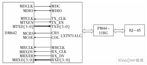
Figure 4 EMAC connection to the underlying network chip
3 terminal workflow
The terminal workflow is shown in Figure 5. At power-on reset, the DM642 performs a reset interrupt to complete initialization of itself and surrounding chips. The external interrupts EXTIN4~EXTIN7 of the DM642 are multiplexed with the GP[7:4] of the GPIO port. When these pins are configured as external interrupt input pins, the interrupt can be enabled by setting the corresponding bit of the interrupt register IER[7:4]. , Trigger mode (rising edge trigger or falling edge trigger, etc.) is set by the interrupt mode register EXTPOL[3:0]. In this design, the related registers are configured as follows: Let the EXTPOL [1:0] =01 register, set the external interrupt EXTIN5 (GP [5]) to the rising edge trigger, and EXTIN4 (GP [4]) to the falling edge trigger. Therefore, the interrupt function corresponding to EXTIN5 executes the wake-up chip, and starts the functions of image acquisition, processing, and transmission; and the interrupt function corresponding to EXTIN4 performs the functions of stopping image acquisition, processing, and transmission, and sets the control status register to CSR [15: 10] =010001 to change the operating mode of the CPU to the power down mode PD1.
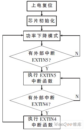
Figure 5 terminal workflow
In the Interrupt Enable Register IER, the IE[15:4] bits are used to enable the CPU interrupt INT[15:4]. When IEx=1, the INTx interrupt response is enabled, and the program's interrupt service function is active. When IEx=0, the INTx interrupt response is disabled. Using the assembly language to set the interrupt bit of the IER register The program code that enables the external interrupt is as follows:
MVK 30H, B1; //B1 register is assigned initial value, corresponding to INT4, INT5
MVC IER, B0; // Assign the current value of IER to register B0
OR B1, B0, B0; //The values ​​in the two registers are ORed by bit.
MVC B0, IER; // Assign the value of B0 register to IER register, IE4, IE5 are set, enable INT4, INT5 If interrupt INT5 is disabled, the following code can be used:
MVK FFDFH, B1; //B1 register is assigned initial value, corresponding to INT5
MVC IER, B0; / / give the current value of the IER register to register B0
AND B1 , B0, B0; // The values ​​in the B0 and B1 registers are "and" in bits, and the result is stored in register B0.
MVC B0,IER // Assign the value of the B0 register to the IER register, IE5 is cleared
When the infrared sensor detects that a person enters the monitoring area, the output end of the infrared sensing signal processing circuit Vo changes from a low level to a high level, and maintains a high level for a period of time. After the rising edge trigger signal is detected on the EXTIN5 (GP[5]) terminal of the DM642, the corresponding interrupt function is executed to wake up the chip and start image acquisition, processing, and transmission functions. Since the infrared sensing signal processing circuit is set to the repeatable trigger mode, as long as there is a person walking in the monitoring area, the output terminal is always kept at a high level, and the terminal always keeps collecting, processing, and transmitting video images. When there is no pedestrian walking in the monitoring area, Vo changes from high level to low level, and enters the low-level blocking time period. EXTIN4 (GP[4]) end executes the corresponding interrupt after detecting the falling edge trigger signal. Function, stop image acquisition, processing, transmission and other functions, and turn the CPU's working mode into power down mode PD1 again.
This paper is aimed at real-time image processing, adopts the modular design idea, and takes the multimedia dedicated DSP processor TMS32ODM642 as the core. Under the close cooperation of infrared sensor, image acquisition chip and network data processing chip, the terminal can complete image acquisition and processing. The transmission function can adjust the working mode according to the personnel changes in the monitoring area in real time, reduce the processing of useless data, improve the efficiency, save the cost, and meet the social requirements for the green and low carbon of electronic products.
:
Single Stage Oil Lubricated Vacuum Pumps
Oil Vacuum Pump,Air Vacuum Pump,Gast Vacuum Pump,Mini Vacuum Pump
Dongguan Beqile Mechanical&Electrical Equipment CO.,LTD , https://www.betemvacuum.com