The Single Crystal Bottom Plate Development Team of the Diamond Research Center of the Japan Industrial Technology Research Institute (Product Research Institute) has developed a large single crystal diamond wafer manufacturing technology. This technology combines two technologies: a direct wafer technique that directly produces a single crystal of a thin plate-shaped diamond from a seed crystal, and a technique for crystallization large-scale by sequentially changing the growth direction and repeatedly performing vapor deposition synthesis (CVD). . Diamonds have useful properties such as high hardness, high thermal conductivity, wide light transmission wavelength band and band gap, low dielectric constant and excellent chemical stability. Therefore, the electronics industry hopes to use it to fabricate components with properties superior to silicon (Si) and silicon carbide (SiC). However, the technology to mass produce large single crystal diamond wafers has not been established.
In order to solve the above problems, the Research Institute has been studying the synthesis of large single crystal diamonds by microwave plasma CVD since 2003. Up to now, it has been successful in the synthesis of single crystal diamonds of 1 carat size.
The study found that by precisely controlling the surface temperature at around 1200 ° C and accurately controlling the amount of nitrogen added to the reaction gas formed by methane and hydrogen, the growth of abnormal crystals with different orientations can be controlled. In addition, the research institute said that by optimizing the growth conditions of diamond crystals, it is possible to achieve a synthesis of 50 μm/hr which is more than 5 times faster than the original.
This method was applied repeatedly. This technique is characterized by the ability to continue growing with the (100) plane as the growth surface. Initially, the seed crystal having the (100) plane is grown in a rod shape, and then the side surface called the (010) plane is ground, the crystal is grown on the surface, and then the crystal is grown on the (100) plane, thereby gradually crystallizing. Large size. This method can be used to produce a single crystal of 6.6 carats of diamond.
In addition, the Research Institute has developed a direct waferization technology that reduces losses and cuts out the shape of the plate. The direct wafer technology cuts the wafer into a sheet shape with little waste of seed crystals. This time, a 10mm square wafer-like diamond was produced with good reproducibility. The direct wafer technique previously injects a single crystal as a seed crystal before vapor deposition growth, and then introduces a defect layer directly under the surface. After vapor deposition growth, the defect layer forms a graphite structure and can therefore be removed by electrochemical etching. This method loses part of the seed crystal when cutting the seed crystal, but its consumption is only below 1 μm. The seed crystal can be used repeatedly, and the cut wafer can also be used as a seed crystal. This eliminates the need to make ingots and does not require the growth of the back-grinding portion.
Due to the relationship between the CVD devices used, the wafers produced are only 10 mm square. However, in order to expand the possibility of application of diamond semiconductor devices, we will strive to manufacture wafers of 1 inch or more in the future. In the future, we will strive to achieve uniformity and large area by improving the plasma generator, and adopt on-site observation technology to improve the crystal quality.
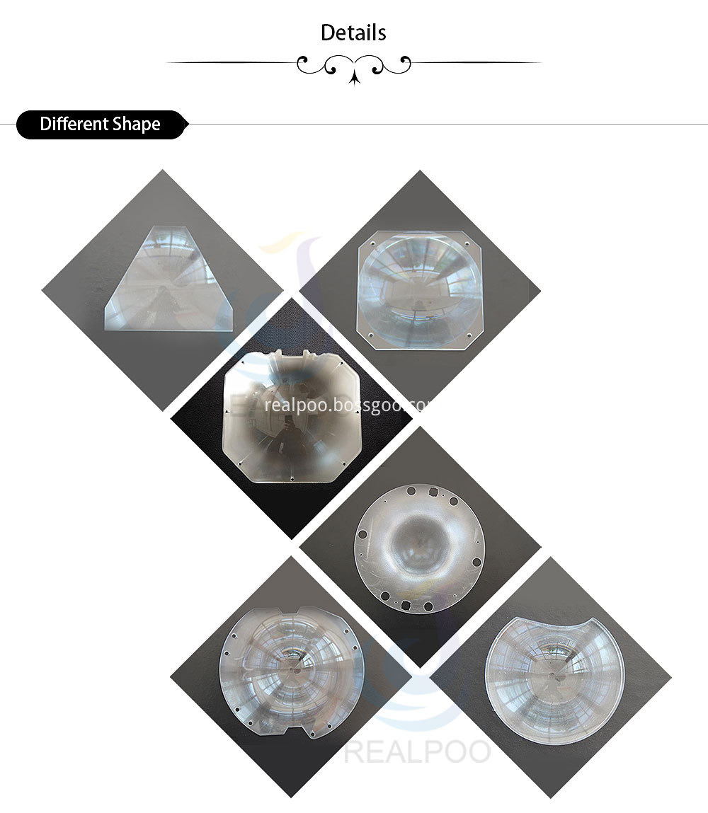
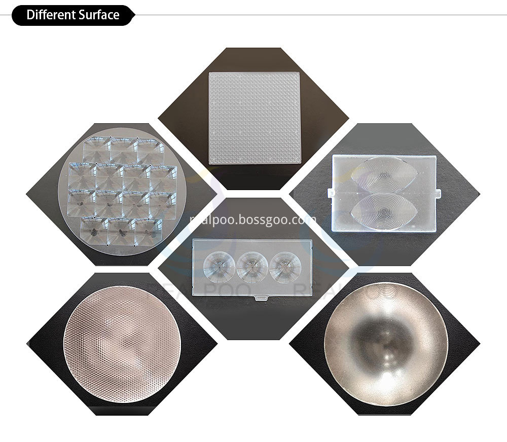
The fresnel lens is a thin sheet made of plastic material. One side of the lens surface is smooth, and the other side is molded with concentric circles from small to large. Its grooves is designed from the interference of light, the relative sensitivity, and receiving angle requirements.
Compared to the conventional Spherical Lens, a Fresnel lens by the lens divided into a series of concentric circles theoretically infinite number of lines (i.e., the Fresnel zone) to achieve the same optical effect, while saving the amount of material For these lines, the overall thickness of the lens is reduced; ordinary Fresnel convex lens is actually a continuous curved surface is truncated to a section of a discontinuous change of the curvature as the surface is finely divided, so look like a
circle around the lines. Fresnel lenses may in fact be regarded as a series of prisms are arranged in a ring, wherein the relatively sharp edge, and the center of the convex surface is relatively smooth.
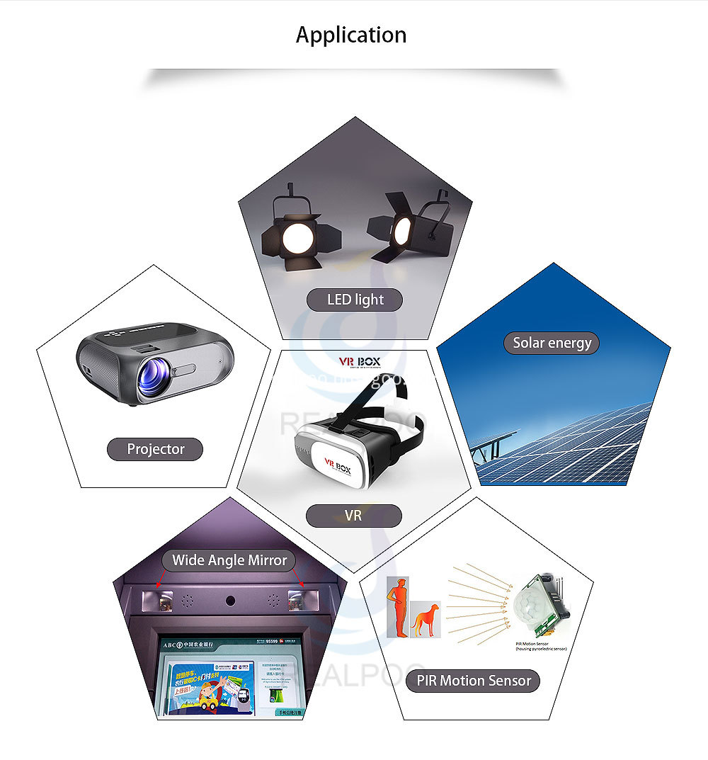
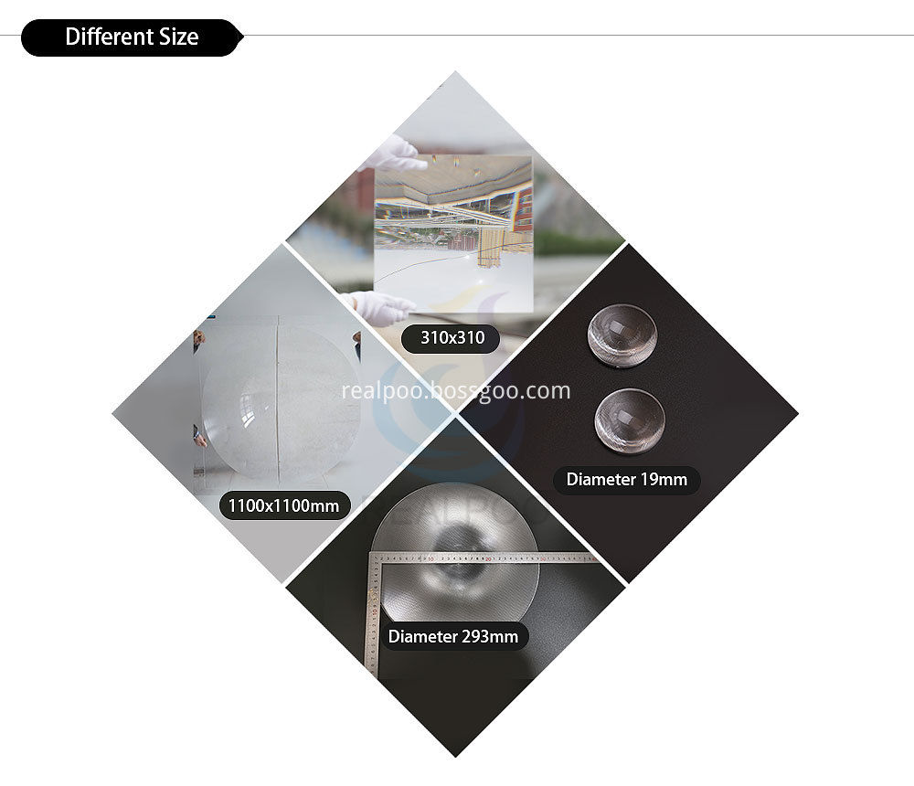
Fresnel lenses are mainly used in optical imaging industry ( projectors, VR, AR, etc.), Fresnel lenses are used in LED lighting distribution (spotlights, floodlights, stage lights, traffic signal lights), infrared induction lenses are used in ( industry 4.0 intelligent fields, building security systems, induction lighting, etc.), large Fresnel lenses are used in ( photovoltaic concentrated light generation, heat collection, light utilization, etc.).


Fresnel Lens,Fresnel Lenses, Led Fresnel Light,Linear Fresnel Lenses,Fresnel Spotlight
Changchun Realpoo Photoelectric Co., Ltd. , https://www.optics-realpoo.com
![<?echo $_SERVER['SERVER_NAME'];?>](/template/twentyseventeen/skin/images/header.jpg)